
 Authorized Dealer
 English
 中文
中文 日本語
日本語






Lenovo’s FC317C is a 65W GaN charger with 2C1A ports. It charges up to three devices at once and delivers 65W from a single port to fast charge laptops and more. With GaN technology and 65W fast charging, this charger delivers high efficiency. Let’s tear it down in detail.
Unboxing of the Lenovo 65W GaN Charger
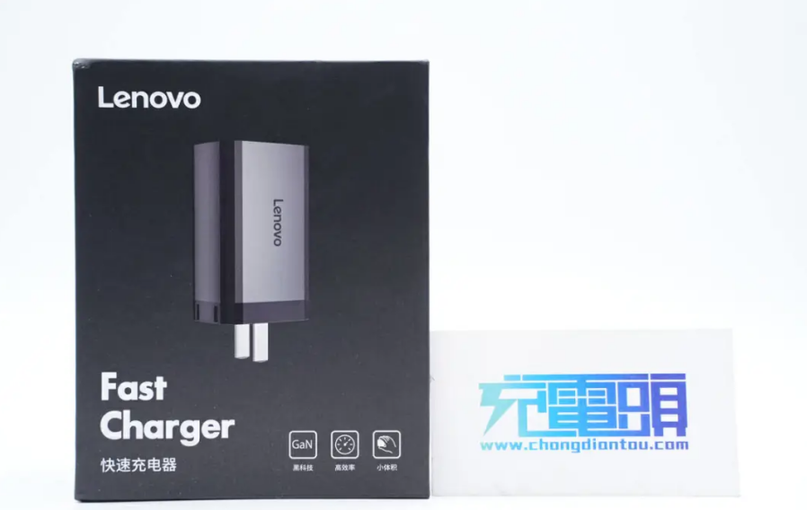
Front: Lenovo logo, charger photo, name, and three key features (GaN, efficiency, small size).
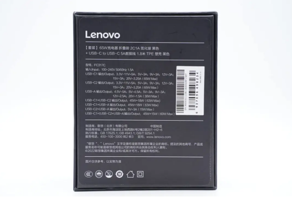 Box: top-and-bottom cover; bottom shows specs and manufacturer info.
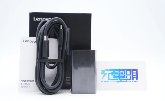
Includes charger, cable, manual.
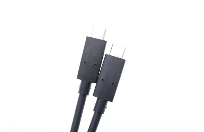 Includes a C-to-C cable with matte-finish connector shells for easy handling; clean design.
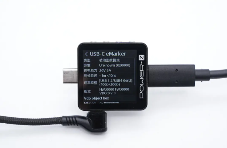 Using ChargerLAB POWER-Z KM003C, the cable shows an E-Marker chip, 20V/5A rating, and supports up to 100W fast charge.
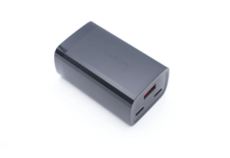 The charger has a column-shaped design.
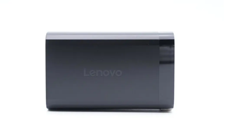
Front center: Lenovo brand logo.
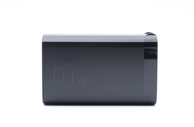
The back of the charger features the text "65W," indicating its output power.
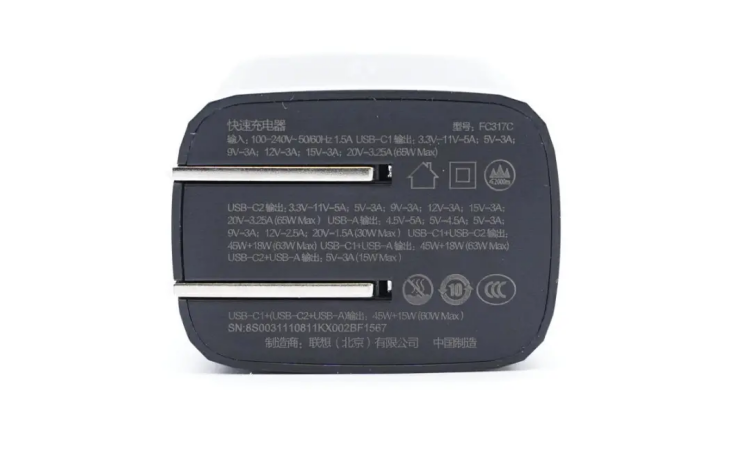
Specs (on input housing):
Model FC317C, Input 100-240V~50/60Hz 1.5A.
Outputs:
C1/C2: 5V3A / 9V3A / 12V3A / 15V3A / 20V3.25A / 3.3-11V5A
A: 4.5V5A / 5V4.5A / 5V3A / 9V3A / 12V2.5A / 20V1.5A
Combo: C1+C2=45+18W(63W max), C1+A=45+18W(63W max), C2+A=5V3A(15W), C1+C2+A=45+15W(60W max).
Mfr: Lenovo (Beijing) Ltd. CCC certified.
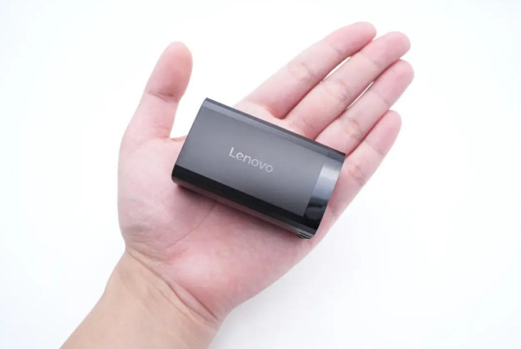
In hand, it feels compact and well-sized.
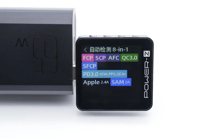
Tested with the KM003C, the USB-C1 port supports the following charging protocols: FCP, SCP, AFC, QC3.0/4+, SFCP, PD3.0, PPS, Apple 2.4A, and Samsung 5V/2A.
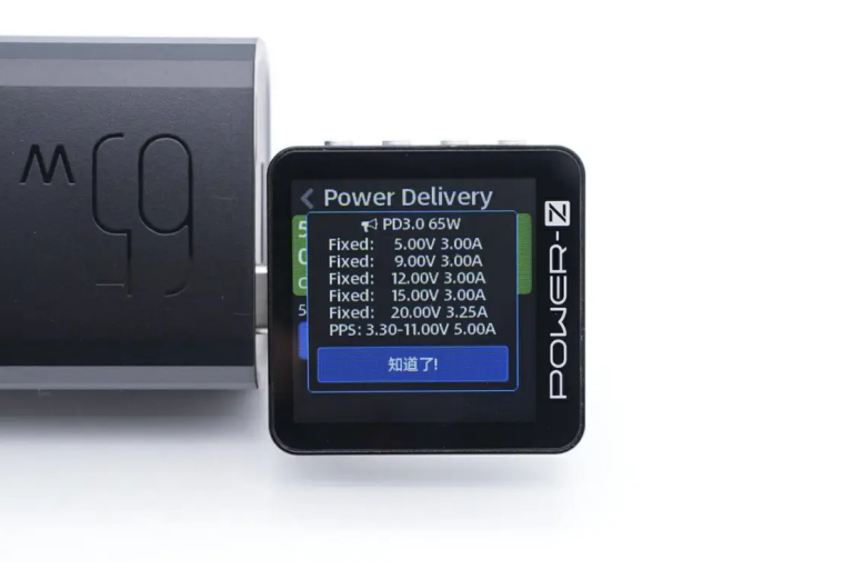
PDO also indicates C1 has five fixed voltage levels (5/9/12/15/20V up to 3.25A) plus a PPS range of 3.3-11V at 5A.
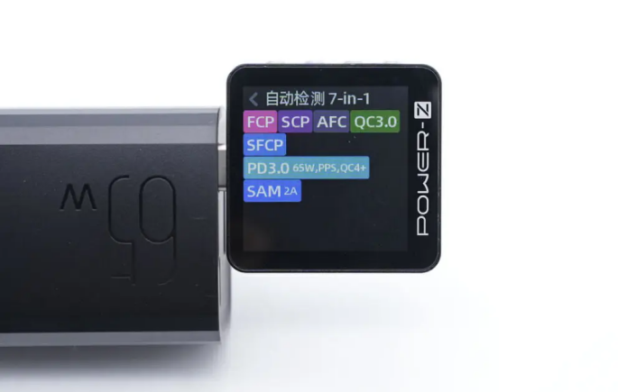
KM003C test shows USB-C2 supports FCP, SCP, AFC, QC3.0/4+, SFCP, PD3.0, PPS, and Samsung 5V2A.
Lenovo 65W GaN Charger Teardown
Having reviewed the looks and test results, let's tear it down to see the internal design and components.
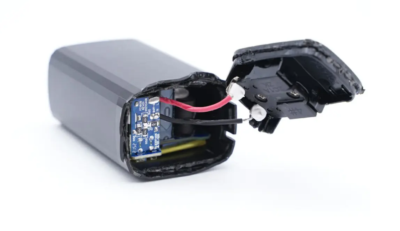
First, detach the foldable plug module along the shell seam. The prongs are soldered to the PCBA via wires.
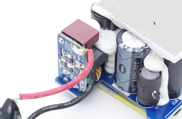
A small PCB is soldered to the input side of the module, which in turn carries the fuse and EMI filter circuitry.
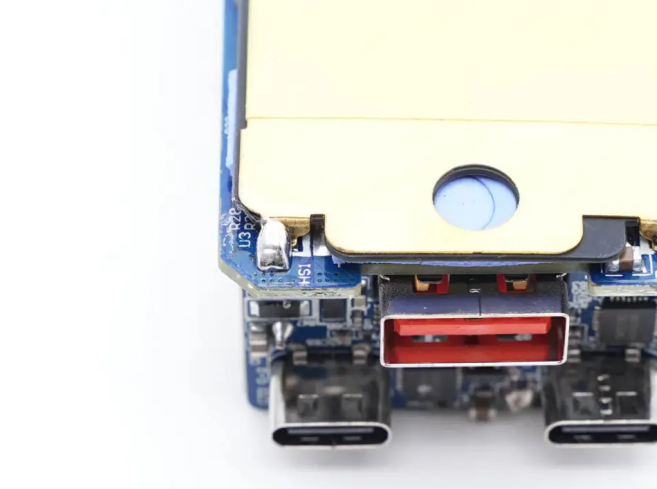
The brass heatsink is fixed by soldering.
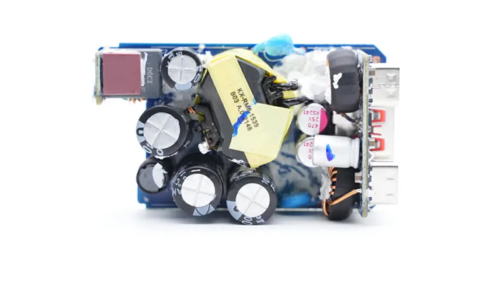
Front view: the PCBA is made up of three soldered boards. Upper left: fuse + EMI filter; to the right: HV filter caps, transformer, and buck board.
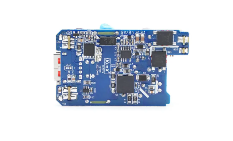
On the back of the PCBA module, the following components are soldered: a synchronous rectification controller, synchronous rectification MOSFETs, a feedback optocoupler, the primary controller IC, a GaN switching transistor, and a bridge rectifier.
The PCBA reveals a flyback design with synchronous rectification and fixed-voltage output. Two independent synchronous buck converters handle the three-port fast-charge output and auto-power allocation.
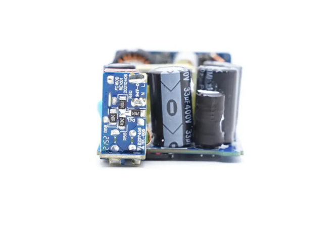
Input side: the small board holds the fuse, X2 cap, and common-mode choke; the main board hosts the HV filter caps and differential-mode inductor.
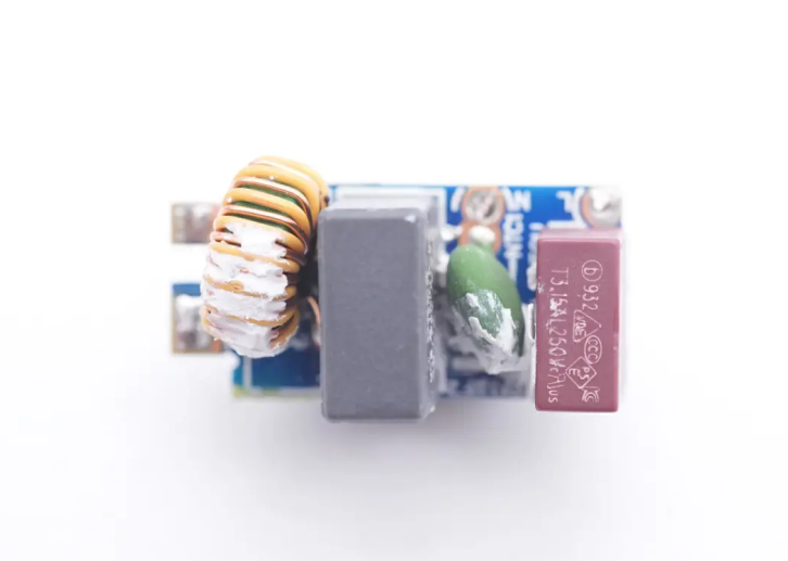
The small board on the input side is populated with a fuse, an NTC thermistor, a safety X2 capacitor, and a common-mode choke.
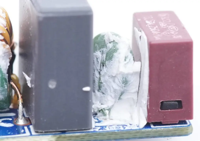
The green NTC thermistor is used to suppress the inrush current when the charger is plugged in.
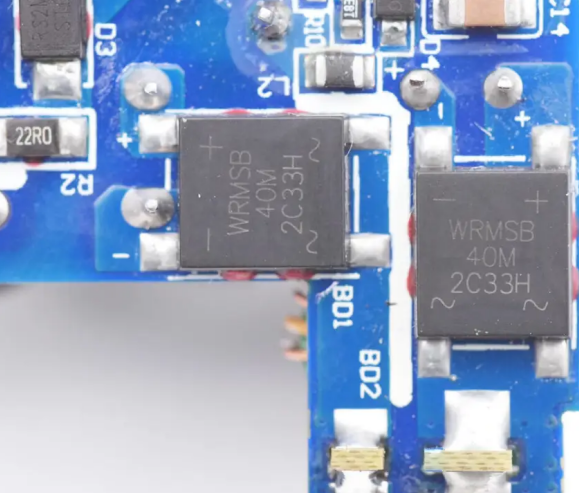
The PCB rear has two WRMSB40M bridge rectifiers in a half-bridge setup to share heat and lower temperature rise. Made by Shenzhen World Industrial, this soft bridge uses a soft recovery curve and smooth turn-off to cut diode junction capacitance and reduce harmonic oscillations.
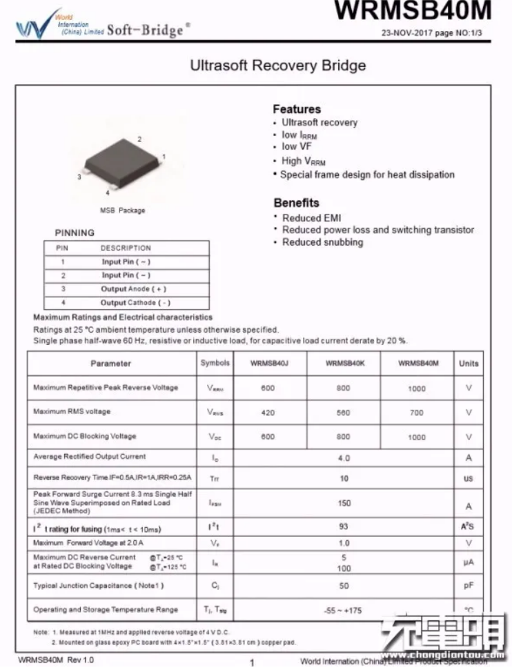
Charging Head Network reports that World's soft bridge is used in many GaN chargers, such as OPPO 50W, Hongdasun 65W, Feipin 65W, ROCK 65W, Maiduoduo 65W, and Maiduoduo 30W 1A1C. The performance has been well recognized by clients.
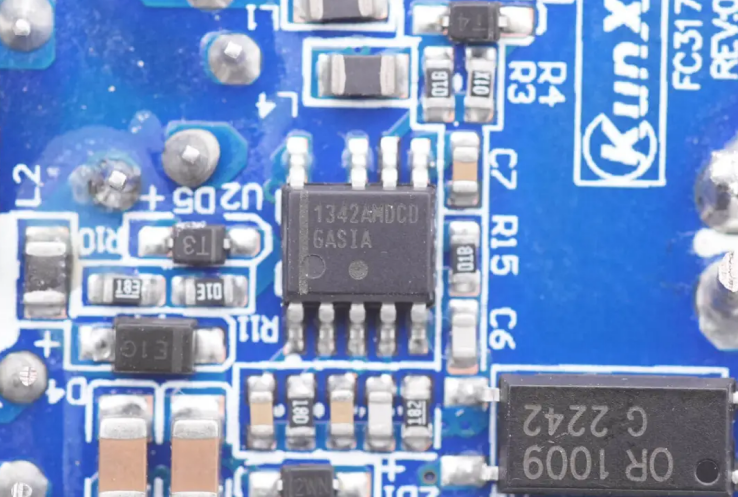
The primary controller utilizes the onsemi NCP1342, a high-frequency quasi-resonant flyback PWM controller. It features integrated active X2 capacitor discharge, a wide VCC operating range, and comprehensive protection mechanisms, including NTC-based overtemperature protection.
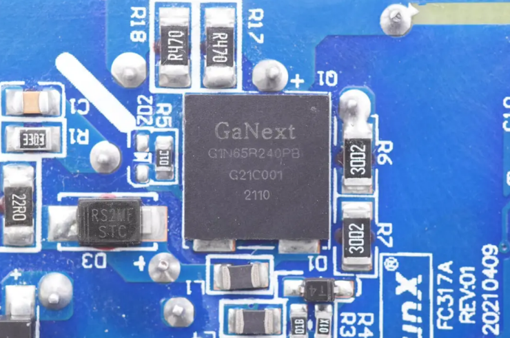
The PFC boost switch is sourced from Zhuhai GaNext (model: G1N65R240PB). It is a 650V GaN power device with a nominal on-resistance (Rds(on)) of 240mΩ and a gate voltage tolerance of ±18V. Being compatible with standard silicon MOSFET drivers, it significantly simplifies the gate drive circuit design compared to enhancement-mode GaN devices.
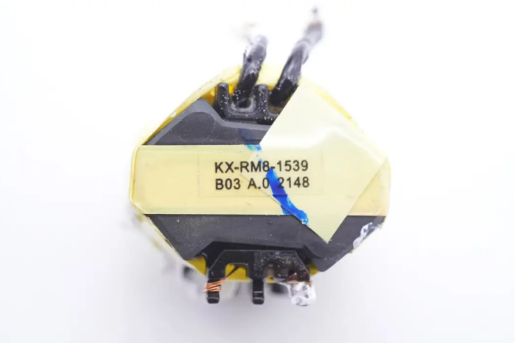
The transformer utilizes an RM8 magnetic core, and the secondary winding is constructed with triple-insulated wire (TIW).
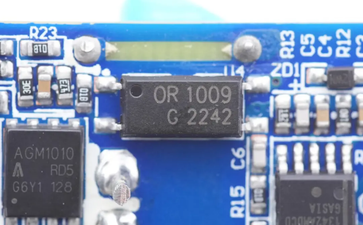
The output voltage feedback loop utilizes the Orient OR1009 optocoupler.
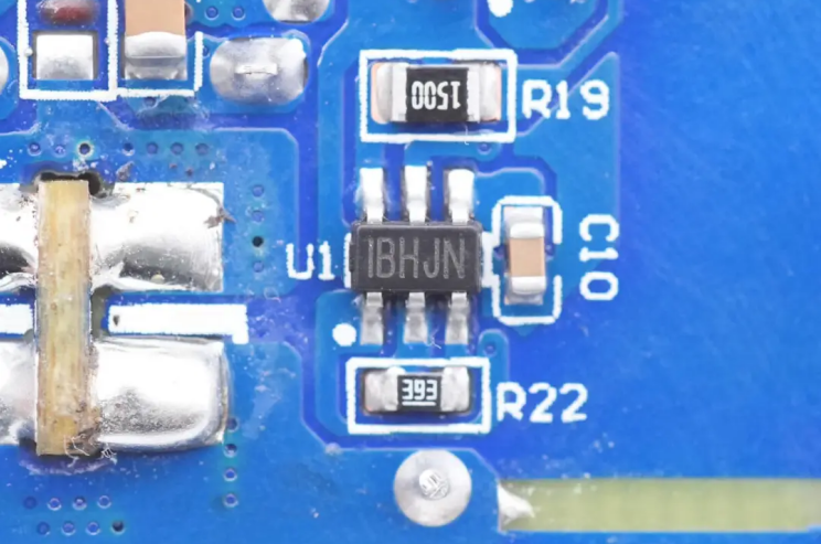
The synchronous rectification controller bears the marking "IBHJN" and is actually the MP6908A from MPS (Monolithic Power Systems). It supports a maximum operating frequency of 600kHz and is compatible with DCM, CCM, QR, and ACF operating modes. The device supports both high-side and low-side applications and features built-in ringing detection to prevent false turn-on.
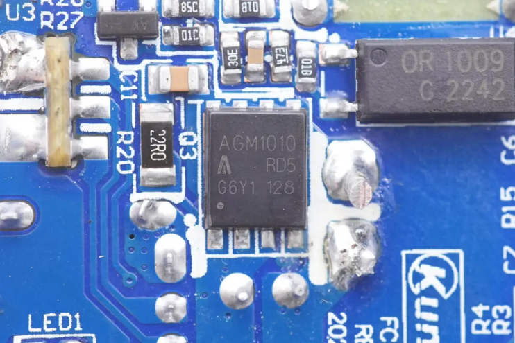
The synchronous rectifier (SR) MOSFET is sourced from AGMSEMI (model: AGM1010). It is a 100V N-channel MOSFET housed in a PRPAK5x6 package.
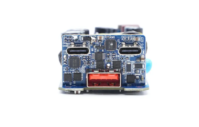
The output end of the charger is equipped with a soldered USB-A female connector and a step-down sub-board. The USB-C female connector and the step-down circuit are mounted on this sub-board.
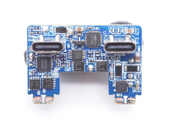
The front side of the sub-board is populated with two step-down controller ICs, synchronous buck switch MOSFETs, and corresponding VBUS switches. It also features an MCU for automatic power control, along with two soldered USB-C female connectors.
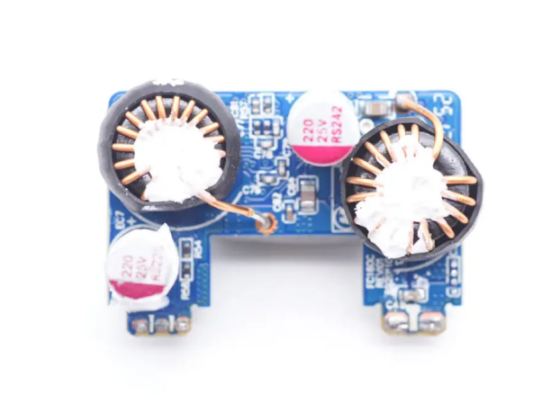
The back side of the sub-board is populated with two step-down inductors and two output filter capacitors.
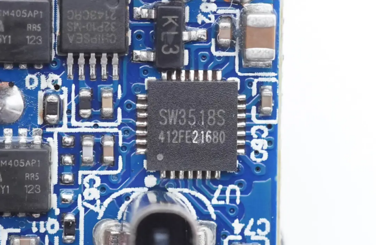
The secondary buck controller is SmartSens' SW3518S, a dual-port fast-charge IC with VOOC certification. It supports flexible output via USB-A or USB-C, independent dual-port current limiting, and an integrated 5A synchronous buck converter. Protocol support includes PPS, PD, QC, AFC, FCP, SCP, PE, SFCP, and VOOC, with PD up to 100W.
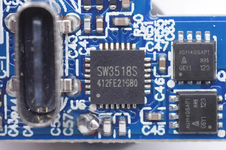
The other step-down controller utilizes the identical model.
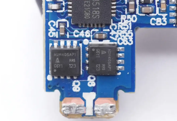
The external synchronous buck converter utilizes two MOSFETs sourced from AGMSEMI (model: AGM405AP1), featuring a 40V voltage rating and a 5.7mΩ on-resistance.
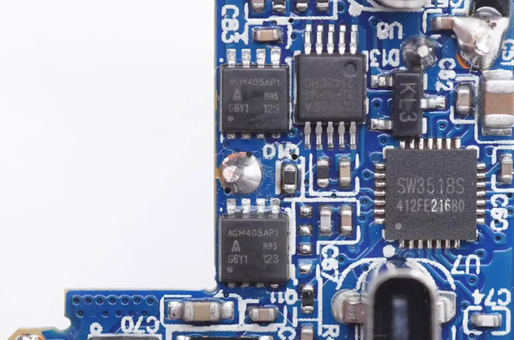
The VBUS switch for the USB-C1 port utilizes the AGM405AP1 from AGMSEMI.
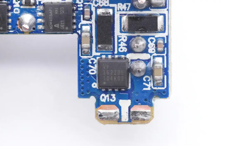
Vango Technologies' VS3622DE dual N-channel MOSFET handles VBUS switching for USB-C2 and USB-A, with 30V, 10mΩ, 5V logic-level drive, and PDFN3333 package.
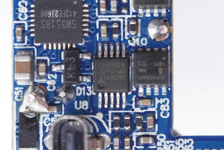
The MCU for automatic output power control is sourced from Chipsensing (model: CSU32P10). It is an 8-bit microcontroller with a built-in 12-bit ADC and an integrated internal oscillator. Operating over a wide voltage range of 2.4V to 5.5V, it is housed in an MSOP10 package.
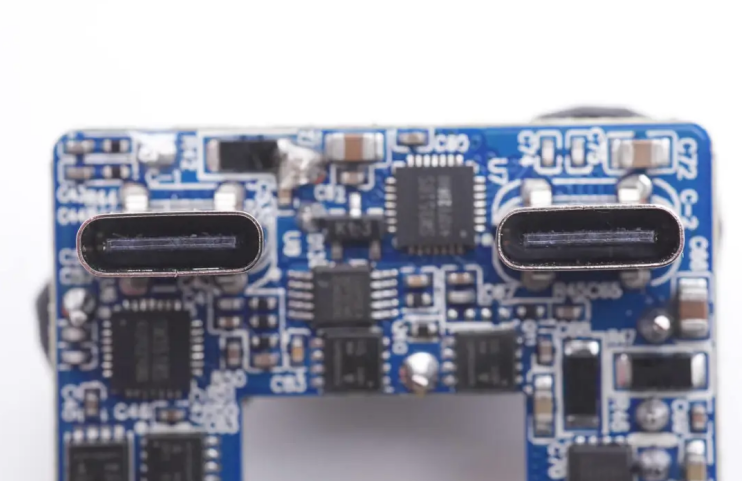
The USB-C female connector features a black plastic housing and is secured through through-hole soldering.
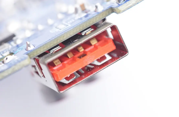
The USB-A female connector features an orange plastic housing. Its widened positive and negative terminals support high-current fast charging, and the front end is equipped with auxiliary contacts.
ChargerLAB Teardown Summary
This 65W GaN fast charger from Lenovo is designed to simultaneously deliver fast charging for devices such as MacBooks and iPhones.
According to ChargerLAB's teardown, the charger utilizes a mainstream high-frequency quasi-resonant (QR) flyback topology, powered by the onsemi NCP1342 controller and the MPS MP6908A synchronous rectifier. It integrates GaNext's G1N65R240PB GaN power device to form a fixed-voltage power supply, which feeds two independent DC-DC step-down circuits.
The secondary step-down stage is driven by the SmartSens SW3518S paired with AGMSEMI MOSFETs for synchronous rectification. Additionally, Vango Technologies VBUS switches are deployed for output control, while a Chipsensing CSU32P10 MCU manages the dynamic output power distribution.